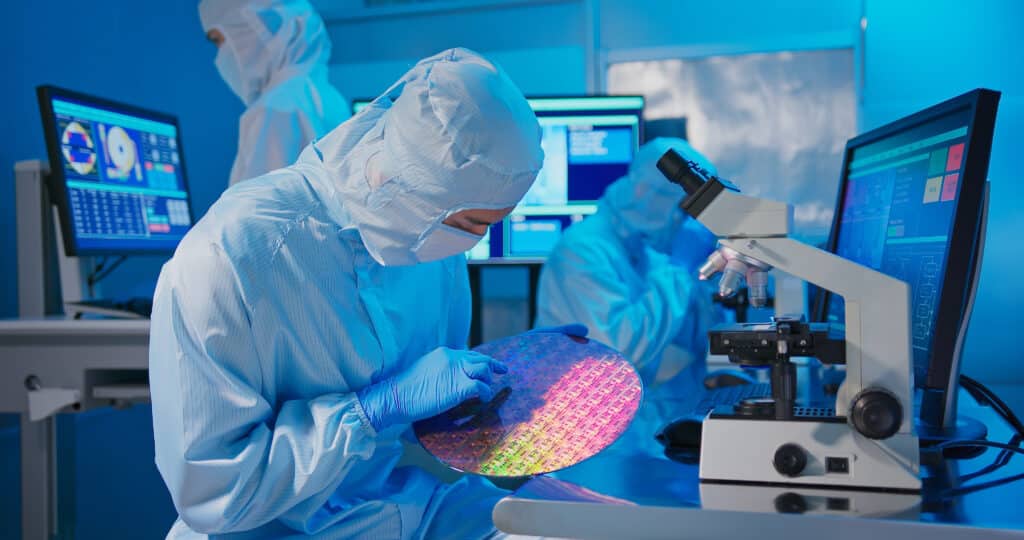
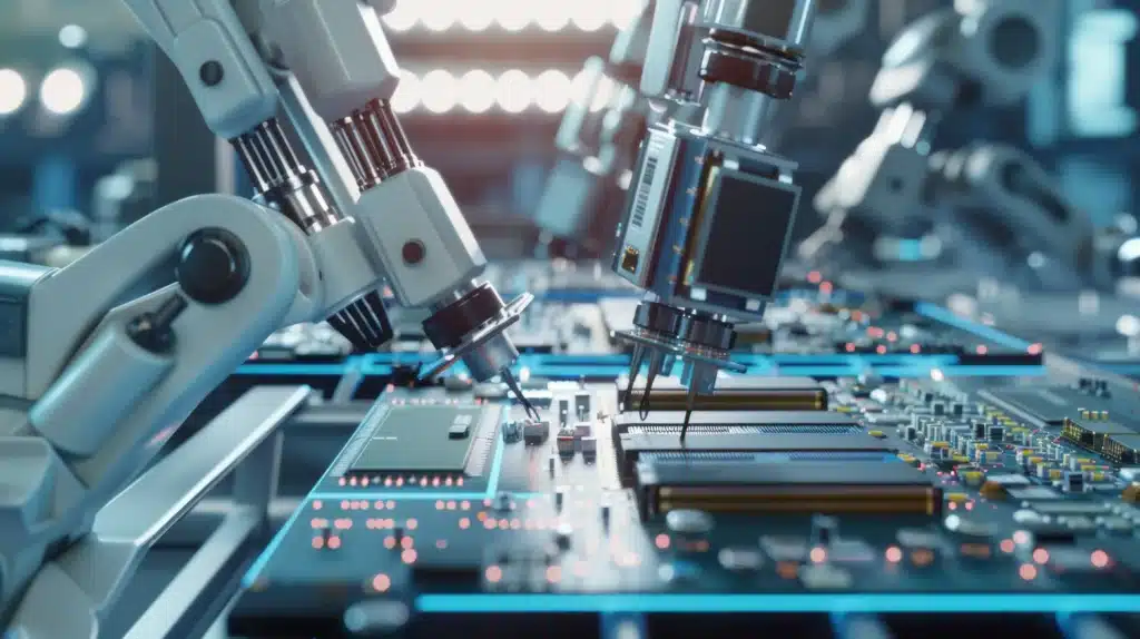
Chip manufacturing, also known as semiconductor fabrication, is a complex and highly specialized field that underpins the functioning of modern electronics. This article explores the detailed steps of chip manufacturing, highlighting advanced methodologies and the latest innovations pushing the boundaries of what is technologically possible.
The Semiconductor Fabrication Process
1. Wafer Production
The journey of a semiconductor chip begins with the production of a silicon wafer. High-purity silicon is derived from silica sand through a series of chemical processes. The Czochralski (CZ) process is typically used to grow monocrystalline silicon ingots. This method involves melting silicon in a crucible, adding a small amount of seed crystal, and slowly pulling the seed upwards while rotating it to form a cylindrical ingot. The resulting ingots are then sliced into thin wafers using a diamond saw. These wafers undergo a series of polishing steps to achieve a mirror-like finish, which is critical for subsequent photolithographic processes.

2. Photolithography
Photolithography is the cornerstone of semiconductor fabrication, enabling the creation of intricate patterns on the wafer surface. This process involves several key steps:
- Photoresist Coating: A spin coater coats the wafer with a light-sensitive photoresist material. The uniformity of this coating is crucial for precise patterning.
- Alignment and Exposure: Using advanced stepper and scanner systems, the wafer is aligned and exposed to ultraviolet (UV) light through a photomask containing the desired circuit patterns. In state-of-the-art facilities, extreme ultraviolet (EUV) lithography, using a 13.5 nm wavelength, allows for patterning at the nanoscale.
- Development: The exposed photoresist is developed, typically using a chemical solution, revealing the patterned areas on the wafer.
3. Etching
Etching removes the unprotected areas of the wafer, transferring the photolithographic pattern into the underlying material. Two main etching techniques are employed:
- Wet Etching involves using liquid chemicals to selectively dissolve unprotected material. This method is often used for simpler patterns and less critical layers.
- Dry Etching utilizes plasma or reactive ion etching (RIE) to achieve highly anisotropic etching profiles, which are essential for fine features. Techniques such as inductively coupled plasma (ICP) and deep reactive ion etching (DRIE) are commonly used for creating deep, narrow trenches and high aspect ratio structures.
4. Deposition
Deposition processes are used to add various material layers to the wafer. Several advanced techniques are employed:
- Chemical Vapor Deposition (CVD) is a chemical process in which gaseous precursors react on the wafer surface to form a solid film. Variants include low-pressure CVD (LPCVD) and plasma-enhanced CVD (PECVD), which offer better control over film properties.
- Physical Vapor Deposition (PVD): This involves vaporizing a solid material (e.g., sputtering or evaporation) and depositing it onto the wafer. Magnetron sputtering is a common PVD technique used to deposit metal interconnects.
- Atomic Layer Deposition (ALD): Provides atomic-scale control over film thickness and composition by exposing the wafer to gas-phase precursors sequentially. This method is essential for depositing ultra-thin, conformal films in advanced nodes.
5. Ion Implantation
Ion implantation is a precise method for doping semiconductor materials. Ions of a dopant element (e.g., boron, phosphorus) are accelerated in an electric field and directed onto the wafer. The depth and concentration of the dopants are controlled by adjusting the ion energy and dose. Post-implantation annealing, typically performed in rapid thermal processing (RTP) systems, is used to repair damage to the silicon lattice and activate the dopants.
6. Chemical Mechanical Planarization (CMP)
CMP is critical for achieving a flat and smooth wafer surface, which is necessary for multi-layer patterning. It involves using a slurry containing abrasive particles, chemicals, and a polishing pad to remove excess material and planarize the wafer. CMP is essential in the fabrication of interconnect layers, where it ensures uniformity and minimizes defects.
7. Metal Interconnects
Creating electrical connections between different parts of the chip involves the deposition and patterning of metal layers. Copper is preferred for interconnects due to its low resistivity and high electromigration resistance. Dual-damascene processes are commonly used to form these interconnects:
- Barrier and Seed Layer Deposition: A thin barrier layer (e.g., tantalum nitride) is deposited to prevent copper diffusion into the silicon, followed by a copper seed layer to promote adhesion and facilitate electroplating.
- Electroplating: Copper is electroplated onto the wafer, filling the vias and trenches etched into the dielectric material.
- CMP: Excess copper is removed using CMP, leaving a planar surface with the embedded copper interconnects.
8. Packaging and Testing
Once the wafer processing is complete, individual chips are separated through dicing. Each chip is packaged to protect it from physical damage and environmental factors. Advanced packaging techniques, such as flip-chip bonding and through-silicon vias (TSVs), enhance performance and integration density. Rigorous testing, including wafer sort and final test, is conducted to ensure functionality and reliability before the chips are shipped to customers.
Current Technologies in Chip Manufacturing
Extreme Ultraviolet Lithography (EUV)
EUV lithography represents a significant leap in photolithography, enabling feature sizes below 10 nanometers. EUV systems use a 13.5 nm wavelength of light generated by a laser-produced plasma (LPP) source. The shorter wavelength allows for finer resolution, but the process is challenging due to the need for high vacuum conditions and specialized optics, such as multi-layer mirrors. EUV masks, made with ultra-thin reflective coatings, are critical components that must be fabricated with atomic precision.
FinFET Transistors
FinFET (Fin Field-Effect Transistor) technology has replaced traditional planar transistors in advanced nodes (e.g., 7 nm, 5 nm). FinFETs have a three-dimensional structure, where the channel is formed along the sides and top of a thin silicon fin. This design improves electrostatic control over the channel, reducing leakage currents and enabling lower threshold voltages. The fabrication of FinFETs involves multiple patterning steps, such as self-aligned double patterning (SADP) and self-aligned quadruple patterning (SAQP), to achieve the necessary fin pitch and alignment precision.
3D ICs and Advanced Packaging
3D integration involves vertically stacking multiple layers of active devices interconnected by through-silicon vias (TSVs). This approach significantly benefits performance, power efficiency, and form factor. Advanced packaging techniques, such as chip-on-wafer-on-substrate (CoWoS) and integrated fan-out (InFO), enable heterogeneous integration of different types of chips (e.g., logic, memory) within a single package. These methods improve signal integrity, reduce latency, and enhance system performance.
Quantum Dots and Nanowires
Researchers are exploring using quantum dots and nanowires to overcome the limitations of traditional semiconductor materials. Quantum dots are nanoscale semiconductor particles with unique electronic properties, enabling quantum computing and optoelectronics applications. Nanowires, with their high surface-to-volume ratio and excellent charge transport properties, are being investigated for next-generation transistors and sensors. Fabrication techniques for these nanostructures include chemical vapor deposition (CVD), molecular beam epitaxy (MBE), and colloidal synthesis.
Challenges and Future Directions
While chip manufacturing has achieved remarkable advancements, it faces ongoing challenges:
Cost and Complexity
Developing and deploying cutting-edge manufacturing technologies, such as EUV lithography, is extremely expensive. Building a state-of-the-art semiconductor fabrication plant (fab) can cost $10 billion. The increasing complexity of chip designs and the move towards smaller nodes require highly sophisticated and precise manufacturing processes, adding to the overall cost and technical challenges.
Material Limitations
As transistor sizes approach the atomic scale, new materials and techniques are needed to maintain performance improvements. The industry is exploring alternatives to silicon, such as silicon-germanium (SiGe) and III-V compounds (e.g., gallium arsenide, indium phosphide), for their superior electron mobility and thermal properties. Integrating these materials into existing fabrication processes presents significant challenges, requiring innovations in deposition, etching, and doping techniques.
Thermal Management
The increasing density of transistors on a chip leads to higher power consumption and heat generation. Effective thermal management is critical to maintaining performance and reliability. Advanced cooling solutions, such as microfluidic and thermoelectric devices, are being developed to dissipate heat efficiently. Additionally, materials with high thermal conductivity, such as diamond and graphene, are being investigated for use in heat spreaders and interconnects.
Quantum Effects
At nanoscale dimensions, quantum mechanical effects become significant, impacting device behavior and performance. Addressing these effects requires new modeling and simulation tools to predict and optimize the performance of nanoscale transistors accurately. Research into quantum computing and quantum-dot cellular automata (QCA) also holds promise for developing fundamentally new approaches to computation that leverage quantum effects for increased performance and efficiency.
Conclusion
Chip manufacturing is a complex, high-precision industry central to modern technology’s functioning. Current advancements such as EUV lithography, FinFET transistors, and 3D ICs enable the production of smaller, faster, and more efficient chips. As the demand for more powerful electronics grows, ongoing innovation and investment in semiconductor fabrication technologies will be crucial in meeting future challenges. For PhD students and researchers in this field, a deep understanding of these processes and technologies is essential for driving the next wave of advancements in chip manufacturing.
Follow MechInsights for Mechanical Engineering Contents.

2 Comments
Pingback: Floating Wind Farms-Interesting Topics For Renewable Energy
Pingback: 3D Printing Technology: Major Breakthrough For Future Mfg